
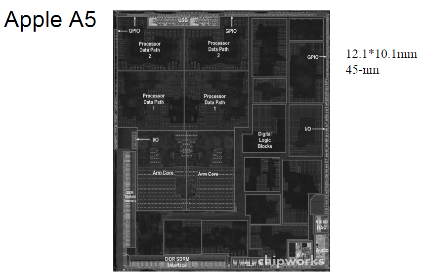
CPU基础知识详解
文章目录
- Abstractions抽象
- 半导体与集成电路
- Semiconductor Technology
- 集成电路发明
- Intel Core i7 Wafer
- Integrated Circuit Cost
- Defining Performance
- Response Time and Throughput
- Relative Performance
- Measuring Execution Time
- CPU Clocking
- CPU Time
- CPU Time Example
- Instruction Count and CPI
- CPI Example
- CPI in More Detail
- CPI Example
- Performance Summary
- Power Trends
- Reducing Power
- Multiprocessors(多核)
- SPEC CPU Benchmark
- SPEC Power Benchmark
- Pitfall(陷阱): Amdahl’s Law
- Fallacy谬误: Low Power at Idle
- Pitfall: MIPS as a Performance Metric
- Concluding Remarks
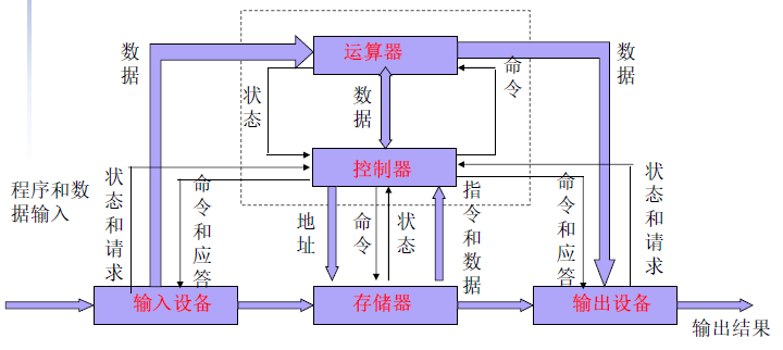
冯·诺依曼计算机
冯·诺依曼计算机由存储器、运算器、输入设备、输出设备和控制器五部分组成。
哈佛结构
哈佛结构是一种将程序指令存储和数据存储分开的存储器结构,它的主要特点是将程序和数据存储在不同的存储空间中,即程序存储器和数据存储器是两个独立的存储器,每个存储器独立编址、独立访问,目的是为了减轻程序运行时的访存瓶颈。哈佛架构的中央处理器典型代表ARM9/10及后续ARMv8的处理器,例如:华为鲲鹏920处理器。
组成计算机的基础硬件都需要与主板(Motherboard)连接
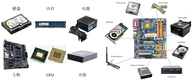
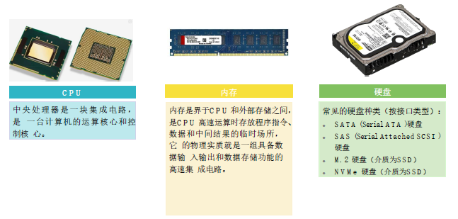
计算机基础硬件 (2)
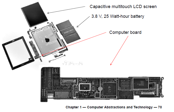
Opening the Box(Apple IPad2)
手机的内部结构 – 华为Mate30 Pro
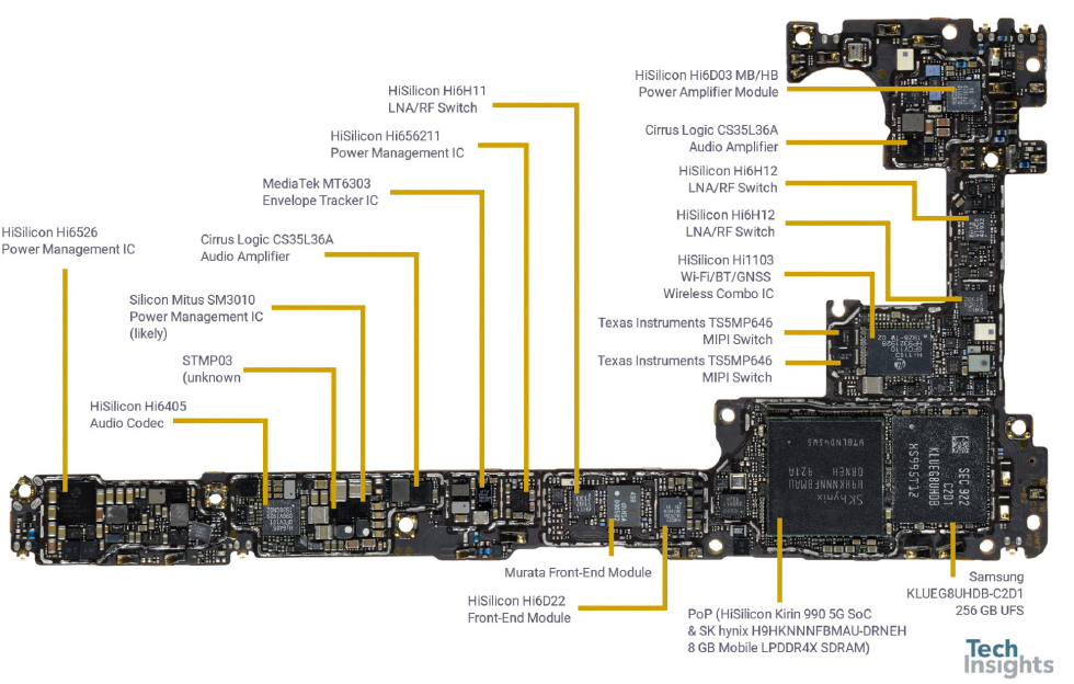
主板(来自于 Tech Insights)
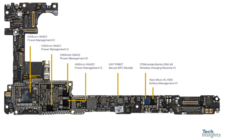
主板 背面
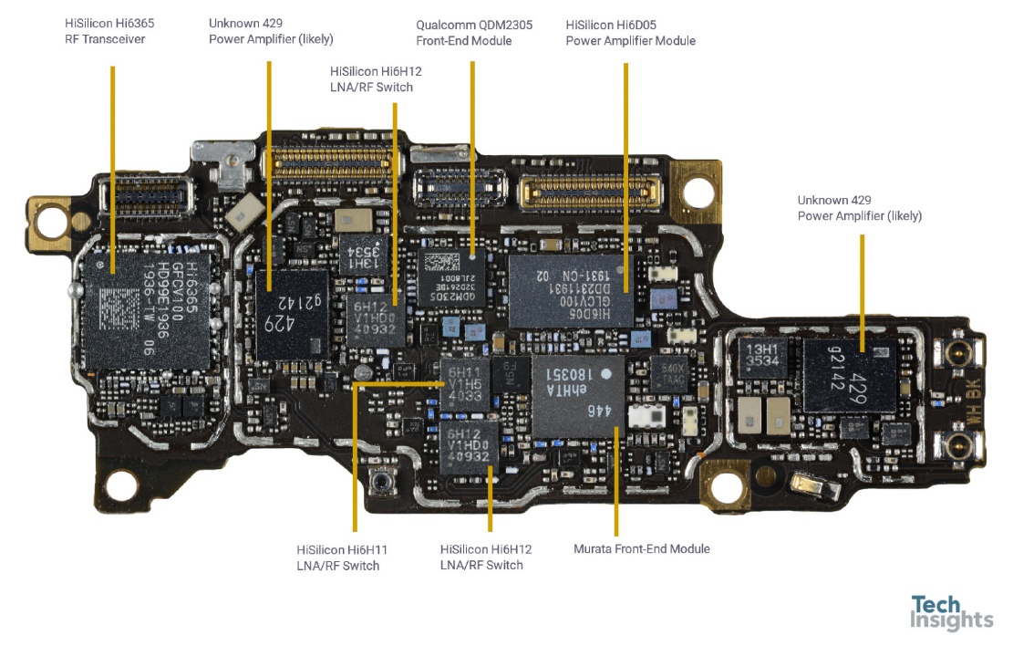
射频板
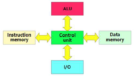
Inside the Processor (CPU)
- Datapath(数据通路): performs operationson data
- Control: sequences datapath, memory, …
- Register 寄存器
- Cache memory 缓存
- Small, fast: SRAM(静态随机访问存储器)
memory for immediate access to data
- Small, fast: SRAM(静态随机访问存储器)
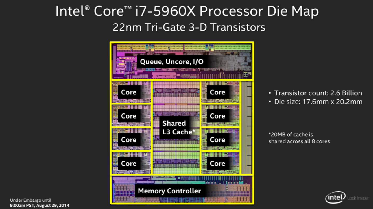
Intel Core i7-5960X
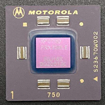
毅力号CPU曝光:250nm工艺、23年旧架构、主频仅233MHz
毅力号搭载的处理器是20多年前技术的产品。处理器型号为PowerPC 750处理器,与1998年苹果出品的iMac G3 电脑同款,PowerPC 750 处理器最高主频速度仅233MHz,且晶体管数量也只有600 万个,但单价仍高达20 万美元(约130万元)。抗辐射、耐寒冷-55~125℃
对比苹果最近推出的M1ARM 架构处理器拥有最高主频3.2GHz,晶体管数量达160 亿个。
处理器发展趋势
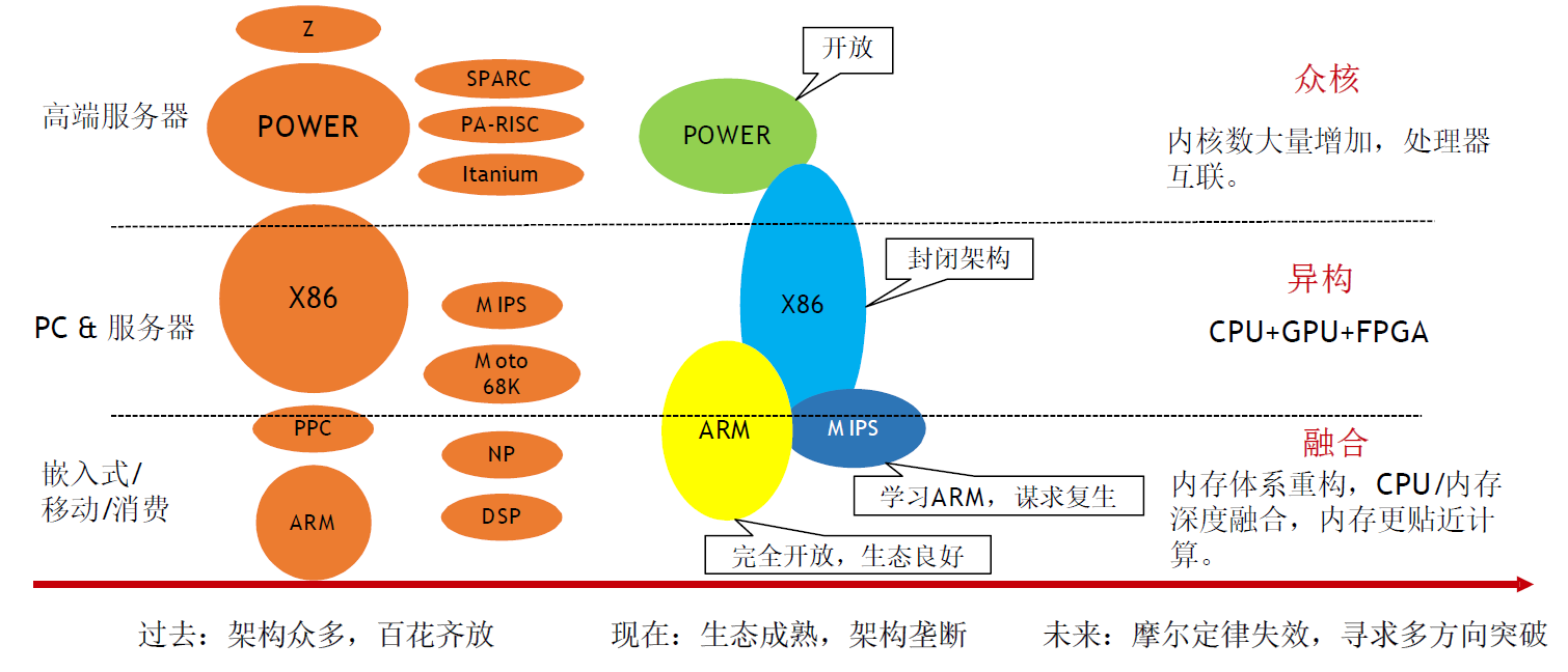
主流CPU发展路径
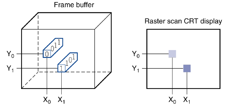
Through the Looking Glass
LCD screen: picture elements (pixels像素)
- Mirrors content of frame buffer memory帧缓冲存储器
Touchscreen(触摸屏)
PostPC device
- Supersedes(取代)keyboard and mouse
- Resistive阻性 and Capacitive容性types
- Most tablets, smart phones use capacitive
- Capacitive allows multiple touches simultaneously(多点同时触控)

A Safe Place for Data
Volatile main memory(易失性主存)
- Loses instructions and data when power off(断电)
Non-volatile secondary memory
- Magnetic disk(磁盘)
- Flash memory(闪存)
- Optical disk (CDROM, DVD) 光盘
Networks 与其他计算机通信
-
Communication(通信), resource sharing(资源共享), nonlocal access(远程访问)
-
Local area network (LAN): Ethernet,局域网/以太网
-
Wide area network (WAN): the Internet,广域网/互联网
-
Wireless network: WiFi, Bluetooth(蓝牙)

计算机基础硬件 (3)
Abstractions抽象
The BIG Picture
- Abstraction helps us deal with complexity
- Hide lower-level detail
- Instruction set architecture (ISA)指令集体系结构
- The hardware/software (abstraction) interface
- Application< ---- > binary interface应用二进制接口
- The ISA plus system software interface
- Implementation(区别于Architecture)
- The details underlying the interface
半导体与集成电路
Technology Trends 处理器和存储器制造技术–趋势
Electronics technology continues to evolve
- Increased capacity and performance
- Reduced cost
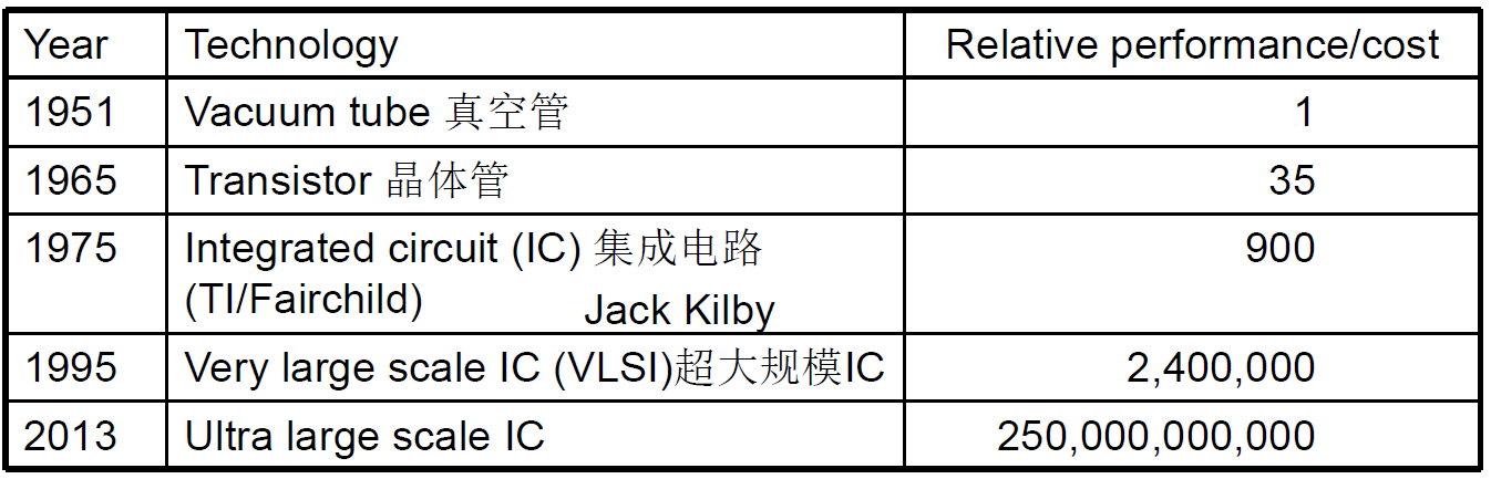
Semiconductor Technology
- Silicon硅: semiconductor 半导体
- Add materials to transform properties属性:
- Conductors
- Insulators
- Switch
设备列表
厂商在制造芯片的过程中,从前端工序、到晶圆制造工序,之后再到封装和测试工序,主要用到的设备依次包括,单晶炉、气相外延炉、氧化炉、低压化学气相沉积系统、磁控溅射台、光刻机、刻蚀机、离子注入机、晶片减薄机、晶圆划片机、键合封装设备、测试机、分选机和探针台等
集成电路发明
-
1952年,英国雷达研究所的科学家达默在一次会议上提出:可以把电子线路中的分立元器件,集中制作在一块半导体晶片上,一小块晶片就是一个完整电路,这样一来,电子线路的体积就可大大缩小,可靠性大幅提高。这就是初期集成电路的构想。
-
1956年,美国材料科学专家富勒和赖斯发明了半导体生产的扩散工艺,这样就为发明集成电路提供了工艺技术基础。
-
1958年9月,美国德州仪器公司的青年工程师杰克·基尔比(Jack Kilby),成功地将包括锗晶体管在内的五个元器件集成在一起,基于锗材料制作了一个叫做相移振荡器的简易集成电路,并于1959年2月申请了小型化的电子电路(Miniaturized Electronic Circuit)专利(专利号为No.31838743,批准时间为1964年6月26日),这就是世界上第一块锗集成电路。
-
2000年,集成电路问世42年以后,人们终于了解到他和他的发明的价值,他被授予了诺贝尔物理学奖。诺贝尔奖评审委员会曾经这样评价基尔比:“为现代信息技术奠定了基础”。
-
1959年7月,美国仙童半导体公司的诺伊斯,研究出一种利用二氧化硅屏蔽的扩散技术和PN结隔离技术,基于硅平面工艺发明了世界上第一块硅集成电路,并申请了基于硅平面工艺的集成电路发明专利(专利号为No.2981877,批准时间为1961年4月26日。虽然诺伊斯申请专利在基尔比之后,但批准在前)。
-
基尔比和诺伊斯几乎在同一时间分别发明了集成电路,两人均被认为是集成电路的发明者,而诺伊斯发明的硅集成电路更适于商业化生产,使集成电路从此进入商业规模化生产阶段。
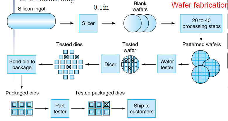
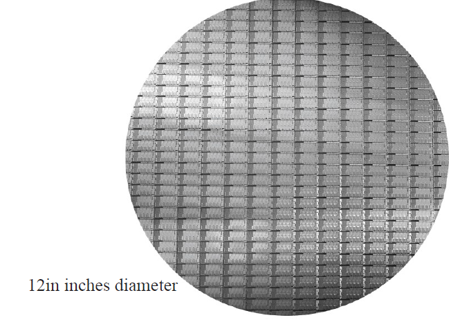
Intel Core i7 Wafer
- 300mm wafer, 280 chips, 32nm technology
- Each chip is 20.7 x 10.5 mm
Integrated Circuit Cost
Costperdie=Cost per wafer Dies per wafer ×Yield Cost per die =\frac{\text { Cost per wafer }}{\text { Dies per wafer } \times \text { Yield }}Costperdie= Dies per wafer × Yield Cost per wafer
Diesperwafer≈Waferarea/DieareaDies per wafer \approx Wafer area/Die areaDiesperwafer≈Waferarea/Diearea
Yield=1(1+(Defects per area ×Die area /2))2Yield =\frac{1}{(1+(\text { Defects per area } \times \text { Die area } / 2))^{2}}Yield=(1+( Defects per area × Die area /2))21
成品率
Defects per area:单位面积缺陷
Die area:模具面积
Defining Performance
- Which airplane has the best performance? 从不同的方面进行考察。
Response Time and Throughput
- Response time响应时间
- How long it takes to do a task(the time between the start and completion of a task)
- Throughput吞吐量
- Total work done per unit time
- e.g., tasks/transactions/… per hour
- How are response time and throughput affected by
- Replacing the processor with a faster version? 改善处理器
- Adding more processors to do separate tasks? 添加更多的处理器
- Queue ?采用排队机制,改善吞吐量
- We’ll focus on response time for now…
Relative Performance
Define Performance = 1/Execution Time
- “X is n time faster than Y”
- $Performance _{X} / Performance _{Y}
= Execution time _{Y} / Execution time _{X}=n $
Example: time taken to run a program
- 10s on A, 15s on B
- Execution TimeB / Execution TimeA = 15s / 10s = 1.5
- So A is 1.5 times faster than B
Measuring Execution Time
- Elapsed time 消逝时间
- Total response time, including all aspects
- Processing, I/O, OS overhead, idle time
- Determines system performance
- Total response time, including all aspects
- CPU time(共享时,独自占用CPU时间)
- Time spent processing a given job
- Discounts I/O time, other jobs’ shares
- Comprises user CPU time and system CPU
time - Different programs are affected differently by
CPU and system performance
- Time spent processing a given job
CPU Clocking
Operation of digital hardware governed(掌控) by a constant-rate clock (数字同步电路)
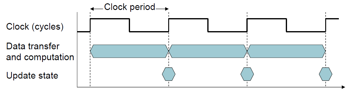
- Clock period: duration of a clock cycle
- e.g., 250ps = 0.25ns = 250×10^–12s
- Clock frequency (rate): cycles per second
- e.g., 4.0GHz = 4000MHz = 4.0×10^9Hz
CPU Time
CPU Time = CPU Clock Cycles x Clock Cycle Time =CPU Clock Cycles Clock Rate \frac{\text { CPU Clock Cycles }}{\text { Clock Rate }} Clock Rate CPU Clock Cycles
Performance improved by
- Reducing number of clock cycles
- Increasing clock rate
- Hardware designer must often trade off(折中)clock rate against cycle count
CPU Time Example
- Computer A: 2GHz clock, 10s CPU time
- Designing Computer B
- Aim for 6s CPU time
- Can do faster clock, but causes 1.2 × clock cycles
- How fast must Computer B clock be?
ClockCyclesA=CPUTimeA×ClockRateAClock Cycles _{A}= CPU Time _{A} \times Clock Rate _{A}ClockCyclesA=CPUTimeA×ClockRateA
=10s×2GHz=20×10910 \mathrm{~s} \times 2 \mathrm{GHz}=20 \times 10^{9}10 s×2GHz=20×109
=1.2×20×1096s=24×1096s=4GHz\frac{1.2 \times 20 \times 10^{9}}{6 \mathrm{~s}}=\frac{24 \times 10^{9}}{6 \mathrm{~s}}=4 \mathrm{GHz}6 s1.2×20×109=6 s24×109=4GHz
Instruction Count and CPI
ClockCycles=InstructionCount×CyclesperInstructionClock Cycles = Instruction Count \times Cycles per InstructionClockCycles=InstructionCount×CyclesperInstruction
CPUTime=InstructionCount×CPI×ClockCycleTimeCPUTime = Instruction Count \times CPI \times Clock Cycle TimeCPUTime=InstructionCount×CPI×ClockCycleTime
=Instruction Count ×CPIClock Rate =\frac{\text { Instruction Count } \times \mathrm{CPI}}{\text { Clock Rate }}= Clock Rate Instruction Count ×CPI
- Instruction Count for a program
- Determined by program, ISA and compiler
- Average cycles per instruction
- Determined by CPU hardware
- If different instructions have different CPI 指令具有不同CPI
- Average CPI affected by instruction mix
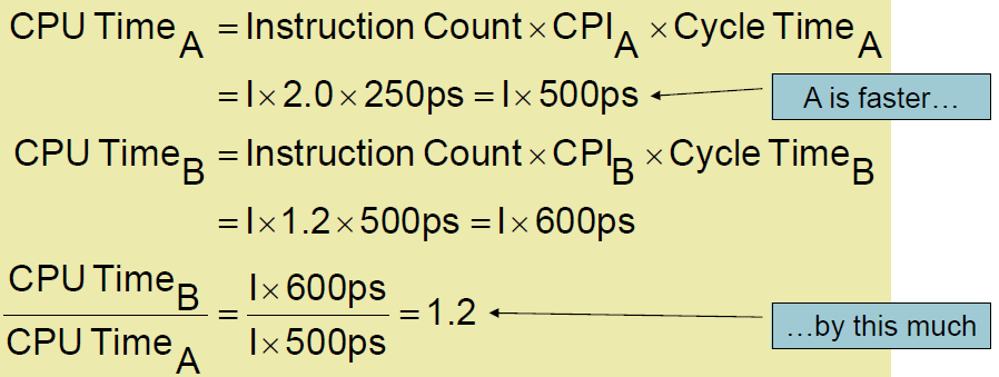
CPI Example
- Computer A: Cycle Time = 250ps, CPI = 2.0
- Computer B: Cycle Time = 500ps, CPI = 1.2
- Same ISA
- Which is faster, and by how much?
CPI in More Detail
If different instruction classes take different numbers 每指令类CPI不同,且指令出现频率不同
Clock Cycles =∑i=1n(CPIi×Instruction Count i)\text { Clock Cycles }=\sum_{\mathrm{i}=1}^{n}\left(\mathrm{CPI}_{\mathrm{i}} \times \operatorname{Instruction~Count~}_{\mathrm{i}}\right) Clock Cycles =∑i=1n(CPIi×Instruction Count i)
Weighted average CPI(平均CPI)
CPI=Clock Cycles Instruction Count =∑i=1n(CPIi×Instruction Count iInstruction Count )\mathrm{CPI}=\frac{\text { Clock Cycles }}{\text { Instruction Count }}=\sum_{\mathrm{i}=1}^{\mathrm{n}}\left(\mathrm{CPI}_{\mathrm{i}} \times \frac{\text { Instruction Count }_{\mathrm{i}}}{\text { Instruction Count }}\right)CPI= Instruction Count Clock Cycles =∑i=1n(CPIi× Instruction Count Instruction Count i)
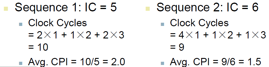
CPI Example
Alternative compiled code sequences using instructions in classes A, B, C (三类指令)
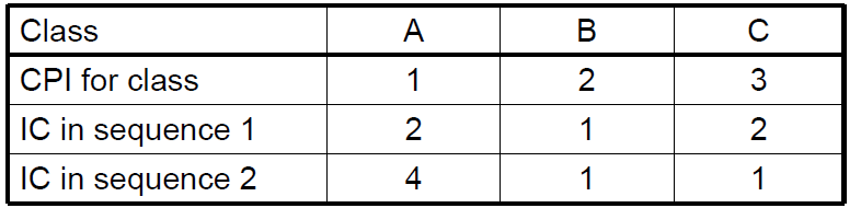
Which code sequence executes the most instructions? sequence2
Which will be faster?
What is the CPI for each sequence?
Performance Summary
CPU Time =Instructions Program ×Clock cycles Instruction ×Seconds Clock cycle \text { CPU Time }=\frac{\text { Instructions }}{\text { Program }} \times \frac{\text { Clock cycles }}{\text { Instruction }} \times \frac{\text { Seconds }}{\text { Clock cycle }} CPU Time = Program Instructions × Instruction Clock cycles × Clock cycle Seconds
Performance depends on
- Algorithm: affects IC(指令数), possibly CPI
- Programming language: affects IC, CPI
- Compiler: affects IC, CPI
- Instruction set architecture: affects IC, CPI, Tc
Power Trends
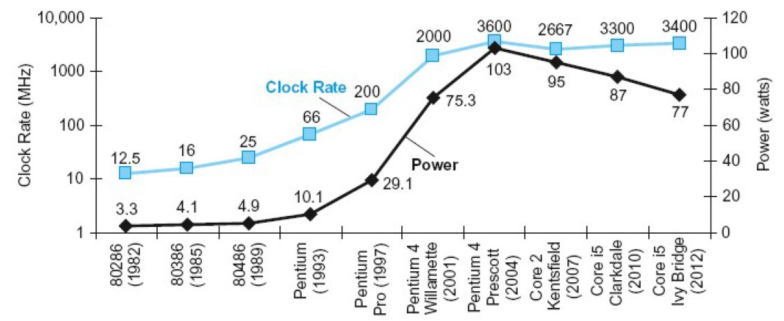
In CMOS IC technology
Power =12Capacitive load ×Voltage 2×Frequency \text { Power }=\frac{1}{2} \text { Capacitive load } \times \text { Voltage }^{2} \times \text { Frequency } Power =21 Capacitive load × Voltage 2× Frequency
Capacitive load:负载电容。
Reducing Power
Suppose a new CPU has
- 85% of capacitive load of old CPU
- 15% voltage and 15% frequency reduction
Pnew Pold =Cold ×0.85×(Vold ×0.85)2×Fold ×0.85Cold ×Vold 2×Fold =0.854=0.52\frac{P_{\text {new }}}{P_{\text {old }}}=\frac{C_{\text {old }} \times 0.85 \times\left(V_{\text {old }} \times 0.85\right)^{2} \times F_{\text {old }} \times 0.85}{C_{\text {old }} \times V_{\text {old }}^{2} \times F_{\text {old }}}=0.85^{4}=0.52Pold Pnew =Cold ×Vold 2×Fold Cold ×0.85×(Vold ×0.85)2×Fold ×0.85=0.854=0.52
- The power wall (功率墙)
- We can’t reduce voltage further 可能低压泄露
- We can’t remove more heat 可能sleep
- How else can we improve performance?
Constrained by power, instruction-level parallelism, memory latency(受到功率、指令级并行性、内存延迟的制约)
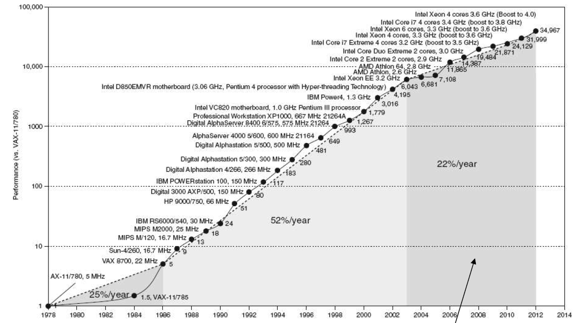
Multiprocessors(多核)
- Multicore microprocessors
- More than one processor per chip
- Requires explicitly parallel programming
- Compare with instruction level parallelism(e.g.流水线)
- Hardware executes multiple instructions at once
- Hidden from the programmer (程序员不可见)
- Compare with instruction level parallelism(e.g.流水线)
- Hard to do
- Programming for performance 编程难度增加
- Load balancing 负载均衡
- Optimizing communication and synchronization
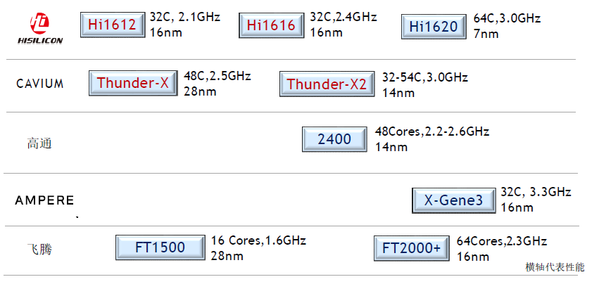
A R M提供更多计算核心
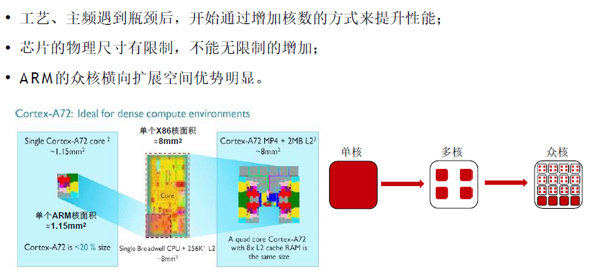
多核架构单位芯片面积提供更强算力,更符合分布式业务的需求
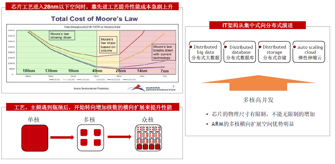
A R M多核高并发优势,匹配互联网分布式架构
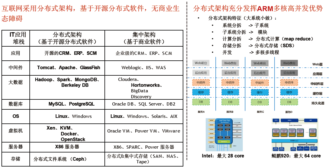
随着多核A R M CPU的性能不断增强,应用领域不断扩展
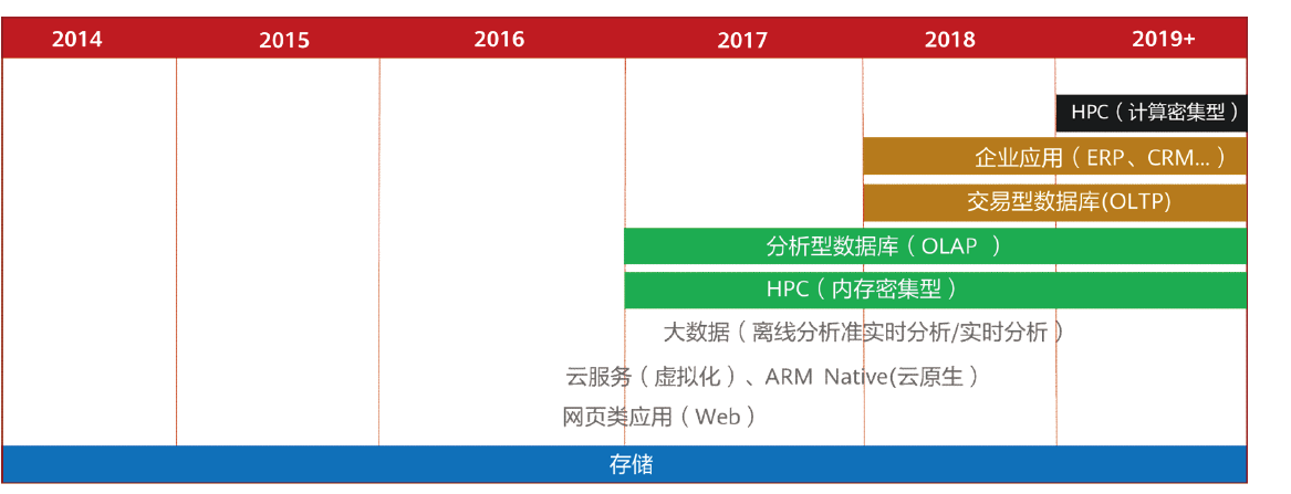
A R M服务器级别处理器一览
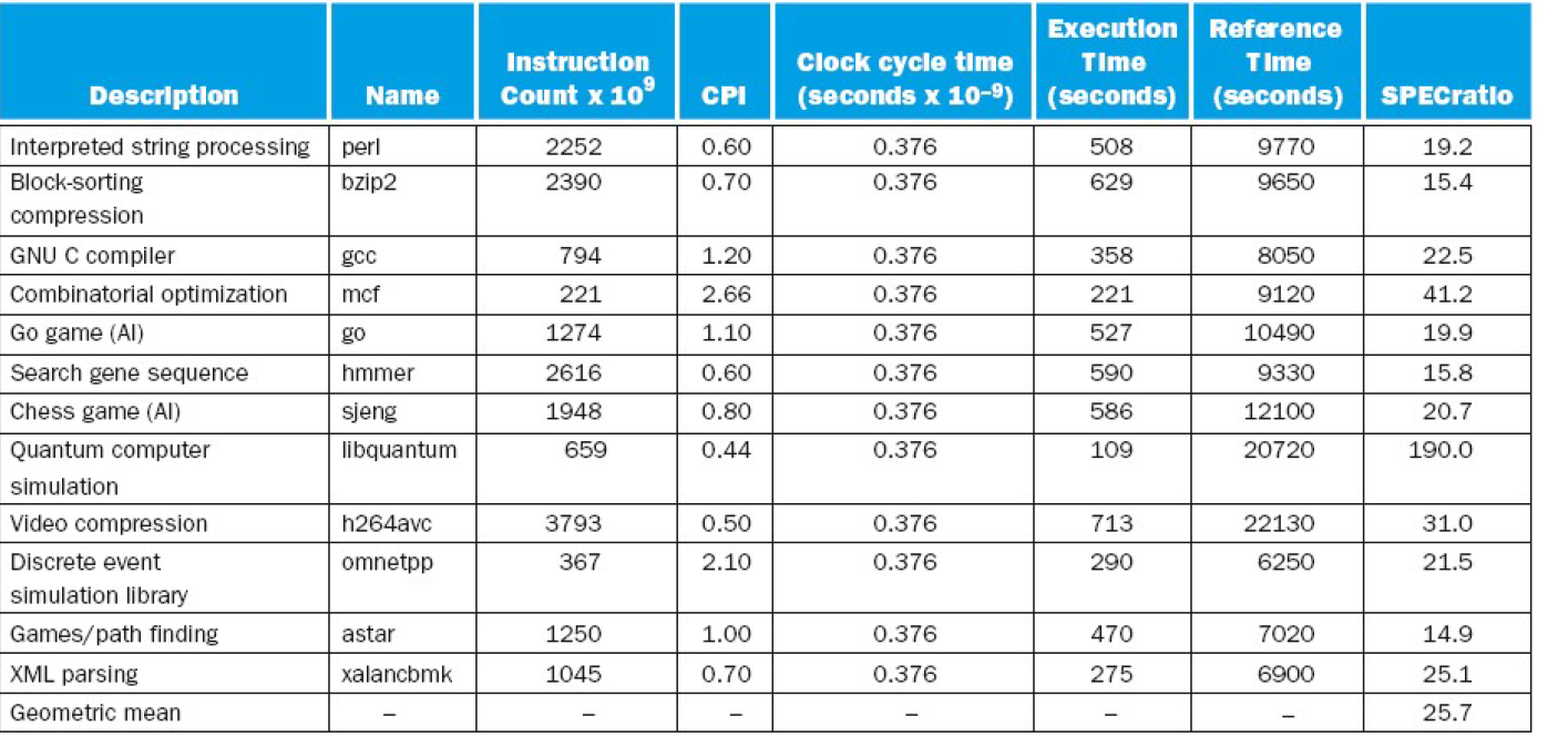
SPEC CPU Benchmark
- Programs used to measure performance
- Supposedly typical of actual workload
- Standard Performance Evaluation Corp (SPEC)
- Develops benchmarks for CPU, I/O, Web, …
- SPEC CPU2006
- Elapsed time to execute a selection of programs
- Negligible I/O, so focuses on CPU performance
- Normalize relative to reference machine(参考机器)
- Summarize as geometric mean of performance ratios
- CINT2006 (integer) and CFP2006 (floating-point)
- Elapsed time to execute a selection of programs
∏i=1nExecution time ratio in\sqrt[n]{\prod_{\mathrm{i}=1}^{n} \text { Execution time ratio }_{i}}n∏i=1n Execution time ratio i
CINT2006 for Intel Core i7 920
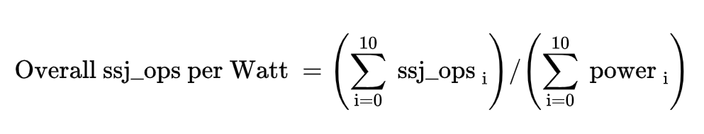
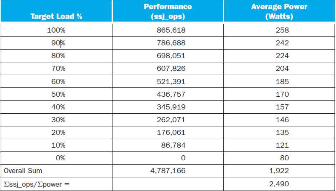
SPEC Power Benchmark
Power consumption of server at different workload levels
- Performance: ssj_ops/sec
- Power: Watts (Joules/sec)
SPECpower_ssj2008 for Xeon X5650
Pitfall(陷阱): Amdahl’s Law
Improving an aspect of a computer and expecting a proportional improvement in overall performance
Timproved =Taffected improvement factor +Tunaffected T_{\text {improved }}=\frac{T_{\text {affected }}}{\text { improvement factor }}+T_{\text {unaffected }}Timproved = improvement factor Taffected +Tunaffected
Example: multiply accounts for 80s/100s
Speedup(E)=1/{(1-P)+P/S}
Amdahl’s law主要的用`途是指出了在计算机体系结构设计过程中,某个部件的优化对整个结构的优化帮助是有上限的,这个极限就是当S->时, speedup(E)= 1/(1-P);也从另外一个方面说明了在体系结构的优化设计过程中,应该挑选对整体有重大影响的部件来进行优化,以得到更好的结果。
Fallacy谬误: Low Power at Idle
Look back at i7 power benchmark
- At 100% load: 258W
- At 50% load: 170W (66%)
- At 10% load: 121W (47%)
Google data center
- Mostly operates at 10% – 50% load
- At 100% load less than 1% of the time
Consider designing processors to make power proportional to load
Pitfall: MIPS as a Performance Metric
MIPS: Millions of Instructions Per Second
-
Doesn’t account for 考虑
- Differences in ISAs between computers
- Differences in complexity between instructions
-
MIPS =Instruction count Execution time ×106=Instruction count Instruction count ×CPIClock rate ×106=Clock rate CPI×106\begin{aligned} \text { MIPS } &=\frac{\text { Instruction count }}{\text { Execution time } \times 10^{6}} \\ &=\frac{\text { Instruction count }}{\frac{\text { Instruction count } \times \mathrm{CPI}}{\text { Clock rate }} \times 10^{6}}=\frac{\text { Clock rate }}{\mathrm{CPI} \times 10^{6}} \end{aligned} MIPS = Execution time ×106 Instruction count = Clock rate Instruction count ×CPI×106 Instruction count =CPI×106 Clock rate
-
CPI varies between programs on a given CPU
Concluding Remarks
Cost/performance is improving
- Due to underlying technology development
Hierarchical layers of abstraction
- In both hardware and software
Instruction set architecture
- The hardware/software interface
Execution time: the best performance measure
Power is a limiting factor
- Use parallelism to improve performance